 English
 Arabic
Against the backdrop of the AI wave sweeping across the globe, computing power has become the most critical technical asset among infrastructure. A single giant currently holds over 80% of the global discrete GPU market share and more than 98% of the data center GPU market share. As we evolve from the A100, H100 and H200 to the B200 and B300 era, export restrictions on high-end computing chips are subjecting domestic computing supply to unprecedented challenges. The domestic substitution of computing chips is no longer merely a choice based on cost and efficiency; it is an imperative consideration concerning industrial chain security and ecological independence.
01.
Industry Definition
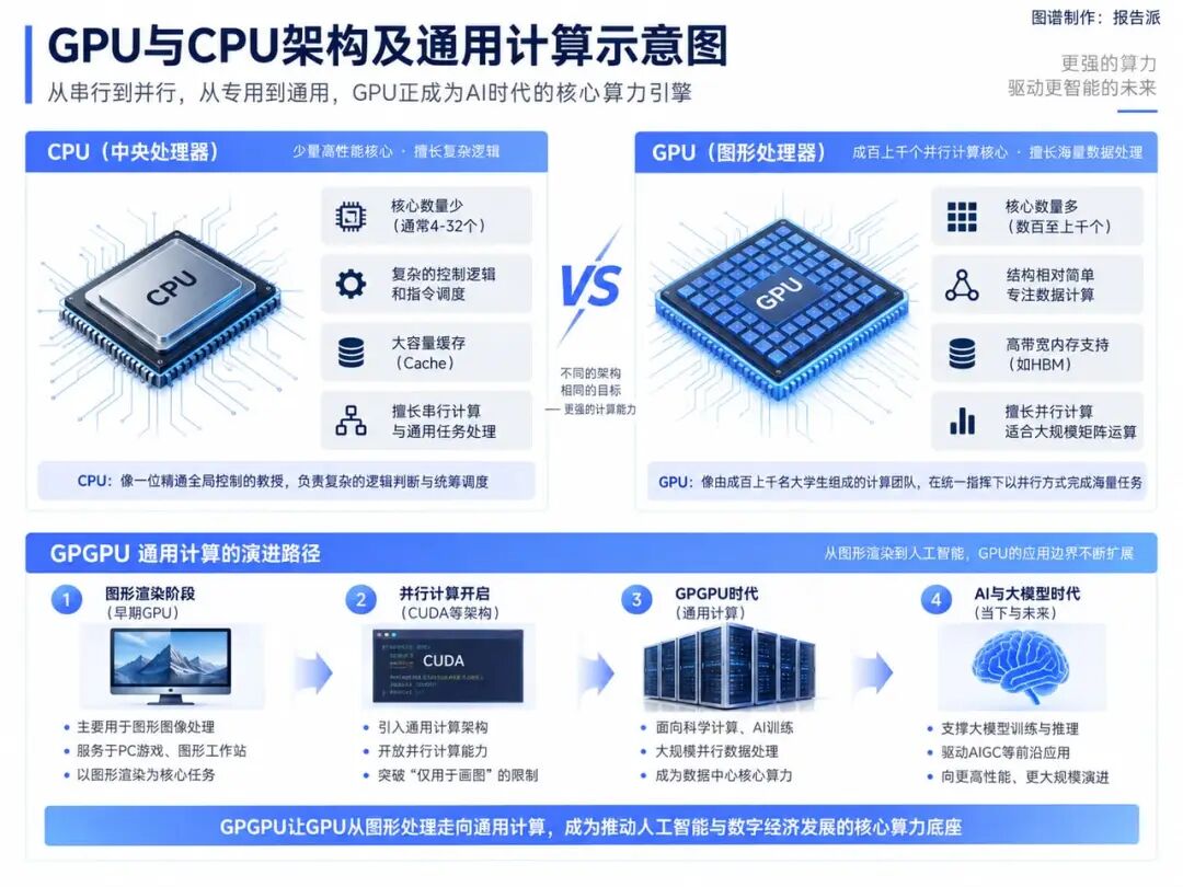
A GPU (Graphics Processing Unit) is a dedicated chip originally developed to handle image and graphics computing, serving as the core component of a graphics card. Thanks to its unique hardware design, a GPU delivers far higher efficiency than traditional processors when processing massive volumes of homogeneous data. This powerful computing capability was later extended to general-purpose computing, giving rise to the GPGPU (General-Purpose Graphics Processing Unit) widely adopted in artificial intelligence and computing hubs today.
Architecturally, a CPU consists of a small number of high-performance cores, excelling at complex logical control and scheduling. By contrast, a GPU is made up of hundreds or thousands of relatively simple cores. If a CPU is likened to a professor skilled in overall control, a GPU is like a large team of college students. Under the unified command of the logic controller, it carries out massive data computing through parallel processing.
02.
Industry Classification
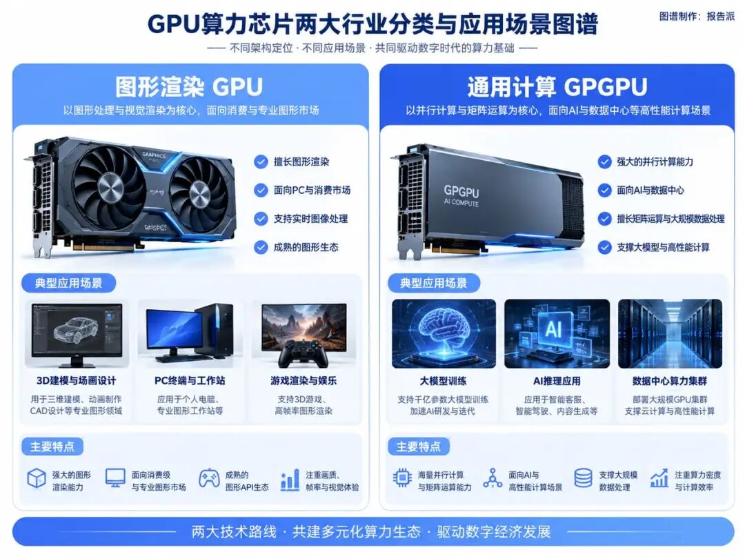
Based on structural form and operational objectives, computing chips in the industry are mainly divided into two core categories:
The first category is traditional graphics-rendering GPUs. Their core capability lies in graphics rendering, 3D modelling and image output, and they mainly serve PC terminals, gaming devices and professional graphics workstations.
The second category is General-Purpose GPUs (GPGPUs). These chips remove or weaken graphics rendering modules and focus on parallel computing and matrix operations for massive datasets. They form the backbone for large model training, deep learning inference and high-density computing in data centers.
03.
Development History
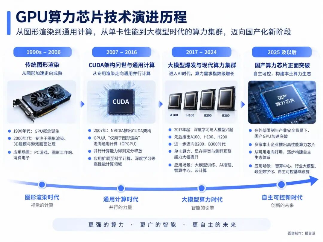
The evolution of computing chips represents a profound shift from "graphics rendering" to "general-purpose computing". Early GPUs were mainly iterated for PC gaming and image processing. It was not until the launch of parallel computing architectures such as CUDA that GPUs broke free from the limitation of being "only for graphics rendering" and entered the realm of high-performance computing.
With the boom of large models and generative AI, computing chips rapidly entered the era of high-density AI computing. Chip giants have dramatically accelerated their iteration pace, rolling out A100, H100 and H200 successively, and further advancing to the B200 and B300 platforms built on more powerful computing architectures. The iteration rhythm and supply constraints of high-performance computing have directly driven domestic computing chips from being a backup option to a stage of breakthrough development.
04.
Full Industrial Chain Overview & Analysis of Upstream, Midstream and Downstream Sectors
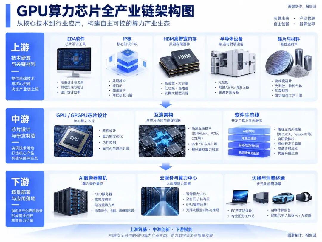
The computing chip industrial chain features extremely high technology intensity and capital intensity. It forms an interconnected industrial cluster covering upstream R&D support, midstream chip design and packaging, and downstream terminal deployment.
Upstream: Technical Foundation & Key MaterialsThe supply capacity of the upstream sector directly determines the performance ceiling and manufacturing feasibility of midstream chip design. First are design architectures and tooling support, including EDA software and underlying IP cores, which are the foundational infrastructure for computing chip design. Second is High-Bandwidth Memory (HBM). For high-end GPGPUs, memory bandwidth is often the key bottleneck restricting the full release of chip computing power. Third are advanced semiconductor materials and manufacturing equipment, including high-purity silicon wafers, photoresist, and wafer-level manufacturing and packaging materials that support high-density integration.
Midstream: Chip Design & Architecture ImplementationThe core of the midstream sector lies in chip design architecture and R&D implementation. In the computing chip space, the competitiveness of midstream enterprises is reflected mainly in two dimensions: hardware performance indicators and ecological compatibility. On the hardware side, enterprises need to address key metrics including computing density, power consumption control and inter-chip interconnect bandwidth. On the software ecosystem side, as international giants have built formidable moats in AI computing, design companies in the midstream generally need to strike a balance between "ecological compatibility" and "self-developed software stacks". This requires chips to match mainstream international performance, alongside an extremely low migration cost for the development toolchain.
Downstream: Scenario Deployment & Commercial ClosureThe downstream sector of computing chips bears heavy pressure for commercial implementation and hosts diverse application scenarios. The first major downstream group comprises computing hubs and cloud service providers. Such customers deploy large-scale GPU clusters and impose stringent requirements on chip stability, energy efficiency and multi-card interconnection performance. The second group includes AI server OEMs, which integrate midstream chips into server systems and deliver standardized computing equipment to government, enterprise, financial and scientific research clients. The third group covers end-user applications and the PC market, including consumer game consoles, professional rendering workstations and edge computing devices.
05.
Landscape of Core Enterprises & Outlook on Independent Controllability
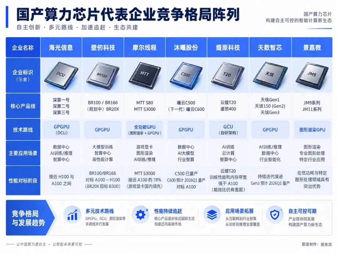
Amid the drive for independent controllability of computing chips, a number of representative domestic enterprises have emerged, pursuing technological breakthroughs across different niche tracks:
Hygon Information: Its DCU products fall under the GPGPU category and support a CUDA-like ecosystem. Three generations of products have been launched: Deep-Sun 1, Deep-Sun 2 and Deep-Sun 3. The performance of Deep-Sun 3 sits between the H100 and A100.
Biren Technology: Focuses on high-end GPGPU R&D. Its flagship BR100 / BR166 delivers performance comparable to the A100–H100 range. The next-generation BR20X under planning targets performance on par with NVIDIA B300.
Moore Threads: Adopts a full-featured GPU technology route. The MTT S80 is the only domestically produced gaming graphics card available for public sale to date. For data center use, its MTT S3000 achieves roughly 78% of the A100’s performance.
Muxi Technology: Specializes in general-purpose GPU computing chips. The Xiyun C500 has entered mass production. Its next-generation Xiyun C600 is scheduled for mass production in Q1 2026, targeting the performance level of NVIDIA A100.
Enflame Technology: Built on the self-developed GCU-CARE architecture. Flagship products include Cloudblaze T20 and Saisi 400. Cloudblaze T20 outperforms the A100 in training computing performance and memory bandwidth, while still lagging in overall energy efficiency.
Iluvatar CoreX: Boasts a clear product iteration roadmap, from Tianji Gen1 to Tianji 150 (Gen2), and Tianji Gen3 planned for mass production in Q1 2026, continuously advancing domestic substitution for high-end training chips.
Jingjiawei: Unlike vendors focused on general-purpose computing, its core products are graphics-rendering GPUs. Its flagship JM9 and JM11 series stand out in low-power consumption and specialized graphics processing.
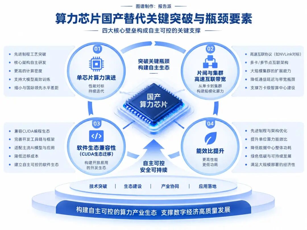
In terms of hardware specifications, domestic computing chips are gradually closing the absolute performance gap with leading international products. Nevertheless, severe technical barriers remain on the path toward independent controllability, covering high-speed interconnection of computing clusters, deep integration of software and hardware ecosystems, and overall energy efficiency.
As hardware performance catches up to the A100 or H100 level, the real challenge for China’s computing industry is not merely whether we can manufacture a single high-performance chip. It is whether we can build an ecosystem and cluster capacity capable of supporting the local AI industry before next-generation architectures become mainstream.

Participate in APCE to Seize Opportunities in the Global Expansion of Modular Data Centers
From March 3–5, 2027, the first APCE Asia Modular Computing Pods, Prefabricated Substations and Associated Products Expo will be held at the Shenzhen World Exhibition & Convention Center (Bao’an).
The exhibition will bring together professional buyers of computing infrastructure from around the world, including IDC operators, cloud service providers, telecommunications carriers, mining and energy companies, international EPC contractors, and overseas infrastructure investment institutions.
By facilitating face-to-face matchmaking for overseas project needs, the event will efficiently shorten the product selection and negotiation process, helping Chinese manufacturers of prefabricated substations, modular computing pods, and related equipment expand into global markets.